Hello,
I´m a newbie from germany, please sorry for my english...
I buy the Spin-1001 DEVB and some FV-1 Reverb IC`s. I want to design some stompboxes for E-guitar. I design my own PCB but the problem is, that I have much noises at the output. I think, it`s a noise about 8-10 kHz and it exist at the output every time. I use the programms from the spin semi webside.
I test miscellaneous V-Reg`s, and some options of filters for the VCC.
If I change the output bypass cap from 2n2 to 220nF, the noise is gone, but this isn`t a option to use it really.
I have a two side PCB, and I have GND Polygons at each sides, should be this the problem ???
thanks for help, and greetings from germany
Saxosun
Output noises / PCB Problem
Moderator: frank
Sounds like a layout problem, please post image of PCB and schematic so we can see how parts are arranged.
What type of power supply are you using? If it is a switching supply that could be the problem.
What type of power supply are you using? If it is a switching supply that could be the problem.
Frank Thomson
Experimental Noize
Experimental Noize
Hello,
thanks for answer.
The power supply is a laboratory power supply ( trafo ), then follows a LF 33 CV.
For a test I try the laboratory power supply directly, and in a other test I try the laboratory power supply -> 7805 -> LF 33 CV, but it`s always the same noise at the output.
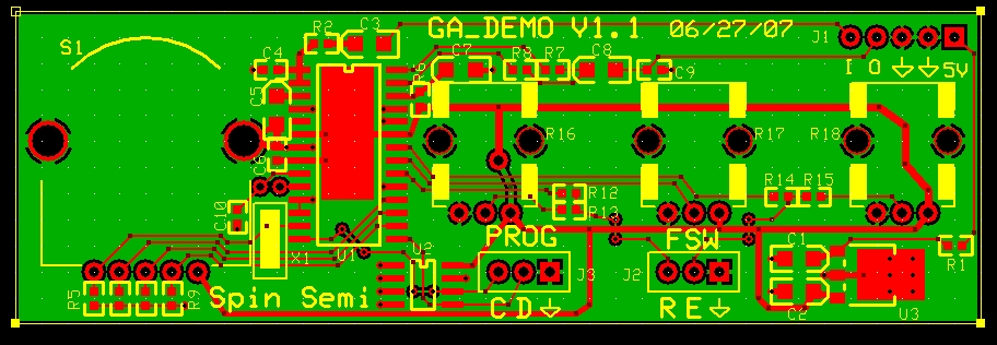
The schematic is the same like this http://www.spinsemi.com/app_download/GA_DEMO_SKE.pdf
Today I will copy this layout http://www.spinsemi.com/app_download/GA_DEMO_PCB.jpg
Where can I post my layout ? I use Eagle for it.
greetings
Saxosun
thanks for answer.
The power supply is a laboratory power supply ( trafo ), then follows a LF 33 CV.
For a test I try the laboratory power supply directly, and in a other test I try the laboratory power supply -> 7805 -> LF 33 CV, but it`s always the same noise at the output.
The schematic is the same like this http://www.spinsemi.com/app_download/GA_DEMO_SKE.pdf
Today I will copy this layout http://www.spinsemi.com/app_download/GA_DEMO_PCB.jpg
Where can I post my layout ? I use Eagle for it.
greetings
Saxosun
Export as a png and post it on a free image hosting site like photobucket or imageshack and put the links to the images here.
Frank Thomson
Experimental Noize
Experimental Noize
OK,
today I design a new Layout. It looks like the Layout from the spin semi webside. I test the circuit, and the noise is much better, but not perfect.
Which devices are much importand from the circuit ? Must I take specific devices for it ??? Low ESR Caps ??? Or an other V-reg ???
greetings Saxosun
today I design a new Layout. It looks like the Layout from the spin semi webside. I test the circuit, and the noise is much better, but not perfect.
Which devices are much importand from the circuit ? Must I take specific devices for it ??? Low ESR Caps ??? Or an other V-reg ???
greetings Saxosun
Here the layout and the schematic. It`s the new one.
http://s812.photobucket.com/albums/zz48 ... ematic.png
http://s812.photobucket.com/albums/zz48 ... bBoard.png
At the pics you see a 7805, but really it`s a LF 33 CV.
http://s812.photobucket.com/albums/zz48 ... ematic.png
http://s812.photobucket.com/albums/zz48 ... bBoard.png
At the pics you see a 7805, but really it`s a LF 33 CV.
Is that a large rectangle under the FV-1 connected to the positive rail?
Frank Thomson
Experimental Noize
Experimental Noize
Hmmm, I do not know why Keith did that, I would not put that large block under the FV-1 connected to power.
The layout looks OK though, you have the caps close to the pins (important pins are 26, 25, 23, 8 and 6 and the cap off the xtal on pin 9)
In general, the exact type of cap should not make a difference. Can you see the noise in other parts of the circuit? Do you see it on the power rails or any of the pins?
Frank Thomson
Experimental Noize
Experimental Noize
Hi Frank,
I detect the power rail, I think nearly the V-Reg it is OK, here a pic:
http://s812.photobucket.com/albums/zz48 ... yV-Reg.jpg
But nearly the FV-1 the noise was bigger, here a pic too:
http://s812.photobucket.com/albums/zz48 ... lyFV-1.jpg
I test some caps at the power rail nearly the FV-1, but it isn`t better.
I will order some SMD parts, so I can design a new layout with all in SMD.
What is the best, the button layer for GND and all other at the top layer ??
No large block under the FV-1 with connecting to power ??, or a large block under the FV-1 with connecting to GND?
I despair
greetings Saxosun
I'm sure there are others who have more experience with pcb layout than me here so hopefully they will post thoughts as well, but...
I like to use the bottom layer for gnd and top for power and signal. If I have to drop to the bottom layer for some short signal runs I will but prefer to not to that with power.
A gnd block under the FV-1 is ok but not really necessary so I've never done it.
Is there anything in the room you are testing in that could be the problem? Lights? Other equipment? Something the traces are picking up?
Frank Thomson
Experimental Noize
Experimental Noize
Hi Frank,
I can´t discover any troublemakers in my room, I test an other room too.
Yesterday I get a new V-Reg, a AS1117, and the noise is a little bit better.
Next week I get my new SMD decives, and I will test a new layout.
If I finished my new design, I will post it.
Thanks a lot for your fast and assistant answers.
greetings Saxosun
What is the power source to the regulator? Does it have much noise?
Frank Thomson
Experimental Noize
Experimental Noize