

|
The FV-1 Architecture overview Before you attempt to program the FV-1, you surely must understand the processor's architecture. Unlike most general purpose DSP chips, the FV-1 has no special setup registers, no 1,000 page manual to digest before anything can be done. The FV-1 however, is really a parallel processor, and coordinating the main process with the LFO generators can be a challenge; hopefully we will be able to make any confusing issues clearer in this document. This is only meant to be a quick overview so that you may become familiar with the FV-1 processor on a rough level before crashing head-on into what would otherwise seem to be a complicated and confusing instruction set. The number of instructions is small, but without an appreciation for the FV-1 architecture and LFO parallel processing, the instruction set could at first seem terribly complicated. In fact, the entire process of programming the FV-1 is quite simple and powerful, once the basic structure is understood. A basic block diagram:
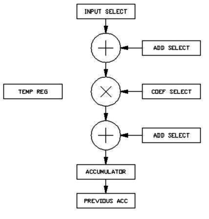
The arithmetic processor is at the heart of the chip, which can access data from the ADC channels, the delay RAM, the register bank and the POT inputs, as well as specific registers within the LFO blocks. The arithmetic block can then output to the DAC, the memories or the LFOs. Control information is either fetched from the internal ROM or the external EEPROM, depending on the state of pin T0. The resolution of the ADC and the DAC is 24 bits, and all processing is done in 24b linear format. The POT inputs are deliberately quantized to 9 bits, with hysteresis added so that potentiometer data does not 'jitter' between adjacent codes. The program counter ranges from 0 to 127, allowing 128 possible process cycles per audio sample. The program can include conditional skip statements however, that allow instructions to be 'skipped over' based on conditions such as accumulator state, but also if the code has executed a previous sample; this allows setup information for LFOs to be imbedded into the program code that is executed only once (as a setup) whereupon the LFOs are left to free-run on subsequent sample cycles. The control store will contain a single complete program, loaded either from the internal ROM or the external EEPROM. Each instruction is 32 bits wide, requiring 4Kb of data per program. Each instruction contains memory address, coefficients and control information as required by the specific instruction. The range of instructions is quite broad, designed to manipulate data most conveniently for audio effects applications. As a result, a single operation may include several simultaneous operations; a multiply and several additions or subtractions contained within a single instruction. As a result, a traditional signal processor would require the execution of several instructions to do the work of a single FV-1 instruction. Signals are delayed in the delay RAM, which is implemented in floating point for increased economy. The address control for the delay memory is calculated from a sample counter plus the relative address that is supplied by a specific instruction, or automatically from an LFO during LFO associated instructions. This allows the pointers that access data within the delay RAM to automatically decrement at each cycle; specific instructions to step to the next memory element on each sample are therefore not required. The processor is further expanded by the inclusion of a logarithm and an exponent block. Single cycles can deliver the LOG or EXP of the previous accumulator value, while scaling the result by a coefficient and adding a constant. This is particularly useful in performing numerical divisions and square roots, as may be required in calculating RMS values of signal amplitudes. The arithmetic process block can be roughly drawn:
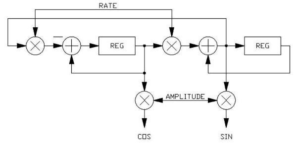
The selectors are instruction controlled to gather several different signal sources to add or subtract with the selected input source, both before and after the multiply, and a multiply coefficient that may be imbedded within the instruction or fetched from the register bank. A temp register holds the last cycle's input value, and a previous accumulator register holds the previous instruction's value. These signals add to the complexity of possible instructions, and the utility of final code sequences. The coefficient width presented to the multiplier will depend on the source. Coefficients imbedded within an instruction are from 11 to 16 bits wide, ranging from -2.0 to +1.999969. The coefficient for interpolation of adjacent samples in a CHO instruction are 14 bits wide, ranging for 0 to 1.0. Values added to the multiplication result during a LOG, EXP or SOF instruction are 11 bits wide. The data representation in all converters and registers is 24bit, 2's compliment, best expressed as: S.bbbbbbbbbbbbbbbbbbbbbbb, in a fractional format. To prevent signal clipping within a program, the ADC signals should be read into the processor at a reduced level, and the algorithm output should then be given corresponding gain when sent out to the DAC. The amount of headroom (if any) required will depend on the program. The result of a LOG operation is shifted 4 places to the right, and the input to an EXP operation is expected to be right shifted 4 places. The LOG operation accepts either positive or negative inputs, and treats them both as positive arguments. Since the maximum input value to the LOG function is 1.0 or less, the LOG result will be zero or negative only. Likewise, the EXP function expects a zero or negative input, positive inputs will produce a saturation limited output. LFOs: The LFOs available within the FV-1 come in two flavors: SIN/COS and RAMP, and two of each are included in the FV-1 structure. These can be used to modulate delays and provide sinesoidally or linearly varying address pointers. The numerical rates (frequency) and amplitudes of the LFOs can be modified by writing new values to them on-the-fly from within a program, but are usually set at the top of the program once, and left to free-run by using the skip operation to jump over the initialization commands. The LFOs provide great flexibility in modulating delays in reverb programs to add spacious variations, or to perform pitch related effects like transposition and flanging. The two styles of LFO are quite different in their structure, but are both capable of simultaneously delivering a relative address to delay RAM while also providing an interpolation coefficient to the arithmetic processor. The CHO instruction (short for chorus) allows direct control of delay memory through an LFO, allowing two successive instructions to access a virtual point within delay RAM, even between RAM locations, effectively providing an automatically, smoothly moving tap from a delay. As can be imagined, the setup for such a process is necessarily complicated. To yet further complicate matters, additional flexibility is found by the choice of SIN or COS outputs to affect delay taps; a quadrature chorus effect is then possible, with very few instructions. The trouble with all of this is that you must first understand the syntax of the LFO setup and use of the rather complicated, yet flexible CHO instruction. The SIN/COS LFO:
A SIN/COS block is a pair of integrators that provide the quadrature signals SIN and COS, at a rate determined by the RATE control signal, and at an amplitude determined by the AMPLITUDE control. These control signals are registers within the SIN/COS block that can be written by a single instruction at the start of the program (and skipped over in subsequent executions) or continuously written by instructions within the program that may be the result of a POT or calculated signal value. The outputs SIN and COS are wide data values that are then split into an integer fraction which can directly address delay memory after being added to the CHO instruction delay address, and a fractional portion that is simultaneously fed as a coefficient to the arithmetic block to perform fractional-location signal interpolation. The CHO instruction has therefore many variables: Which of the LFOs is involved in the operation, whether SIN or COS is used, and whether the operation is on the first memory location or the second location for interpolation. Once you become familiar with the syntax, the process becomes easier to grasp, and of course, examples always help. The RAMP LFO:
The RAMP LFO is a single integrator that is allowed to 'wrap-around', creating a sawtooth waveform. The sign of the RATE control value will determine whether the signal ramps up or down. The numerical derivation allows the calculation of 'crossfade' coefficients that can be selected during a CHO operation to interpolate between the stored output of RAMPA's pointer results to RAMPB's pointer results, allowing a method of pitch transposition. This adds one more possible source of direction for the CHO instruction syntax, that of crossfade control selection. |